Whether you are looking to build a single sided PCB or a multi layer PCB, there are a few things to consider. Those factors include the costs, the automation optical inspection (AOI), and the pad shapes that are used on the inner layers of a PCB.
Single-sided vs multi-layer PCBs
Whether you’re looking to build a single-sided or multi-layer PCB, it’s important to understand the differences and how they can benefit your project. These two types of circuit boards are used in a variety of electronic applications, including household appliances, computers, and calculators.
Single-sided PCBs are made from one layer of conductive metal, called the substrate. They are commonly found in less complex devices, such as printers, household appliances, and calculators. These types of boards are typically easy to produce and can be ordered in large quantities.
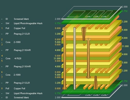
On the other hand, multi-layer PCBs consist of multiple layers of conductive material that are stacked on top of each other. These layers provide added durability and functionality. Despite their advantages, multi-layer boards are usually more expensive and have longer manufacturing times than single-layer PCBs.
The benefits of multi-layer PCBs include more operating capacities, faster speeds, and lower weight. The design is more complex than that of a single-layer board, which means that more planning, skill, and special equipment are needed to manufacture a multi-layer board.
Single-sided vs multi-layer PCB costs
Whether you are trying to design your PCB or are just looking for a better way to do it, you have to decide if a single-sided or multi-layer board is best for you. Which type of PCB you choose will depend on your needs, budget, and capabilities.
If you are working on a simple device, like a printer, calculator, or a small household appliance, a single-sided PCB may be your best bet. It is easier to make and maintain and is usually cheaper than a multi-layer PCB. It also has a few limitations, such as a limited number of connections and lower operating capacity.
On the other hand, a multi-layer PCB is ideal for devices with more complex functions, such as a smartphone. It is smaller, lighter, and can squeeze more functionality into a compact space. It is also durable and can withstand harsh conditions.
You will need to find a specialized company to produce or repair your multi-layer PCB. The process requires advanced equipment and specialized skills. This can increase your lead time and increase your costs.
Pad shapes on inner layer pcb
Whether you’re designing a multi-layer PCB or a single-sided board, pads are a key part of your design. They serve as a designated surface for electrical contacts. They also help to generate a land pattern on your PCB.
Pads and vias can be designed manually or they can be generated automatically. In the manual case, you can draw pad shapes and map them using datasheets and generic pad shape formulas. Using an automated tool can save time.
When you’re designing a PCB, you’ll need to understand the different types of pads. They include through-hole, bottom and surface mount pads. They come in a variety of shapes. Some are even plated.
One of the smallest pad shapes is the teardrop. This shape extends the size of the pad in the direction of the trace. It also does not take up much layout space. It’s a good reflection drill location.
Another pad shape is the annular ring. This ring helps connect the tracing to the hole plating.
Automated optical inspection (AOI)
Using an AOI of a multi layer PCB can help you to detect defects and ensure that your product is in compliance with specifications. Moreover, it can also help you reduce the cost of inspection.
AOI uses a camera to capture images of the product and then process them. It can be used at any stage of the fabrication process. It is a quick way to assess a PCB assembly. Various defects can be detected including surface and dimensional issues, wrong components, and other misalignments.
Earlier AOI machines were equipped with different types of lights, but recent advances in lighting technology have made it possible to create a better image. Today’s equipment also uses cameras that have high resolution. Choosing the right lighting can highlight different kinds of defects.
The AOI of a multi layer PCB will use a machine vision camera to scan the product. The pictures are then processed and compared to the pattern from a “golden board” to determine if there are any defects.